Abstract
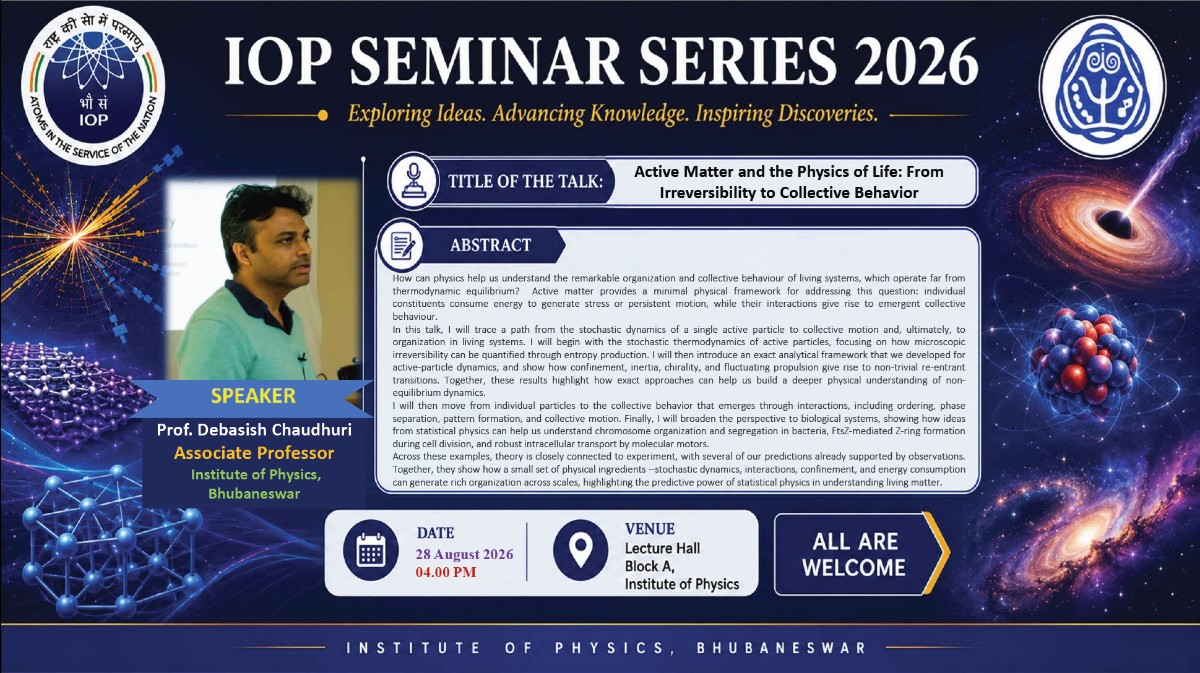
The potential of surface science towards device fabrication isenormous. However, a trivial surface modification of the substratescan sometime alter the morphology and other properties of thesubstrates as well as the over-layer growth significantly. The kineticand thermodynamic control of the growth processes can form stabilizedlayered and nanostructures. I shall discuss about the 2D layers and 3Dnanostructure formation on the semiconductor and insulator substrateslike, Silicon, GaAs and Sapphire. Not only the various new phasediagrams have been proposed but also some of the existing ones arealso modified. We have used the surface chemical and structuralmodification to render substrate compatibility for epitaxial growth.Some of the examples would include the surface modification of GaAssubstrates for initial GaN formation, kinetically controlled selfassembled nanostructures of GaN and the epitaxial growth ofmultilayered and few-layered graphene on Sapphire substrates. Thegrowth of Graphene on insulator can lead to a breakthrough inutilizing insulator substrates as well for the epitaxial growth ofvarious materials like III-Nitrides.



 28-08-2026